

Preface: In an era of intensifying geopolitical rivalry and energetic constraints, China’s latest gallium oxide wafer breakthrough signals more than a materials win — it reveals a sophisticated strategy fusing upstream chemical innovation with systemic industrial power. As part of my ongoing examination of how nations navigate thermoeconomic realities, this development highlights a critical intersection of supply chain mastery, materials science and post-silicon architectures like Tau Law. By scaling ultra-wide bandgap gallium oxide — a superior performer for high-efficiency power electronics — China strengthens control over strategic raw materials while advancing EROEI across electrification and computing stacks. These upstream victories in chemistry and materials do not occur in isolation; they propagate through global value chains, reshaping accumulation regimes and offering alternative development pathways, particularly for the Global South. In a world of “monsters” where energy, technology and geography collide, such breakthroughs underscore the thermoeconomic logic driving today’s great power competition. My hard sciences colleagues may be getting sick of me (!) but I hope their patience is paying off. At the very least, I feel as if I am learning new things. All errors in the essay are mine, of course.
For the lay reader: Imagine semiconductors as the “engines” inside phones, EVs and power grids. For decades, silicon has been the main material, but it struggles with very high voltages and wastes energy as heat. Chinese company Hangzhou Garen Semiconductor just achieved a world first: they built a production line making large (6- and 8-inch) wafers of gallium oxide — a next-generation “super material.” Gallium oxide can handle much higher voltages and runs more efficiently with less waste heat, thanks to its special atomic structure. This is like upgrading from a regular car engine to one that’s far more powerful and fuel-efficient for heavy-duty work. Larger wafers mean cheaper, mass-produced chips for electric vehicles, renewable energy systems, smart grids and 5G / 6G tech. It’s a big step in “post-silicon” electronics, helping China build better power components while reducing energy losses across entire systems. In short: more performance, less waste, and faster progress toward efficient green technology.
Introduction
In the evolving landscape of global technological competition, China’s recent strides in ultra-wide bandgap semiconductors exemplify a deliberate strategy of materials innovation that extends far beyond incremental improvements in computing. The announcement by Hangzhou Garen Semiconductor of the world’s first mass-production line for 6-inch and 8-inch homoepitaxial gallium oxide (β-Ga₂O₃) wafers represents a significant milestone in fourth-generation semiconductor technology. This development not only addresses immediate challenges in power electronics but also contributes to broader gains in Energy Return on Energy Invested (EROEI) at systemic scales. It fits within China’s ongoing R&D emphasis on new materials and chemistry, which collectively strengthen industrial resilience and economic sovereignty.
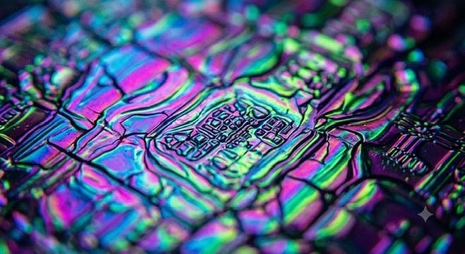
The Scientific Breakthrough
Gallium oxide, particularly in its β-phase, possesses an ultra-wide bandgap of approximately 4.8–4.9 eV — substantially larger than silicon (1.1 eV), silicon carbide (SiC, ~3.3 eV), or gallium nitride (GaN, ~3.4 eV). This enables a critical electric field strength around 8 MV/cm, allowing devices to withstand much higher voltages with lower conduction losses and superior high-temperature performance. Unlike many wide-bandgap materials that rely on heteroepitaxy or complex substrates, Ga₂O₃ supports relatively straightforward bulk single-crystal growth from the melt, facilitating scalable wafer production.
Garen Semiconductor’s achievement builds on proprietary cast-growth techniques for ultra-thick crystals combined with optimised metal-organic chemical vapour deposition (MOCVD) for homoepitaxy. The line supports both 6-inch and 8-inch wafers, with demonstrated delivery of high-uniformity 6-inch (100)-oriented epitaxial wafers (epitaxial layers >10 μm thick, thickness variation <1%). Key process innovations include ultra-thin substrate processing that boosts yield by 3–4 times and drastically reduces iridium consumption (lowering substrate costs by over 80%). Earlier milestones, such as the 8-inch single crystal in 2025, underscore a rapid scaling trajectory, from 2-inch to 8-inch in just a few years.
In its immediate field — high-power electronics — this matters profoundly. Power devices (diodes, transistors, switches) based on Ga₂O₃ promise superior efficiency in electric vehicles (inverters and chargers), renewable energy systems (grid interfaces and storage), data centre power supplies, and RF applications. Higher breakdown voltages reduce the need for bulky cooling and cascading components, while lower losses translate directly to reduced energy dissipation. These attributes position Ga₂O₃ as a strong contender where SiC and GaN are already deployed but face scaling or cost limitations for ultra-high-voltage scenarios.
Systemic EROEI Implications: Vertical and Horizontal Propagation
EROEI improvements arise not just from device efficiency but from propagation through supply chains. Vertically, Ga₂O₃ enhances upstream-downstream linkages: more efficient power conversion in solar inverters or EV drivetrains increases net energy delivered from primary sources (sun, batteries). Reduced material intensity (via higher yields and lower precious-metal use) lowers the energy embedded in manufacturing the semiconductors themselves. As these devices scale into grids and industrial motors, system-level losses decline, amplifying overall EROEI for electrification efforts.
Horizontally, the effects ripple across networks. China’s control over gallium raw materials — combined with integrated domestic chains for crystal growth, substrates, epitaxy, and eventual device fabrication — creates self-reinforcing advantages. This reduces import dependence and vulnerability to supply shocks, stabilising costs and energy inputs for downstream industries (electronics, automotive, renewables). In a global context, it enables technology transfer or licensing to partners, propagating efficiency gains outward. When paired with advances in related materials chemistry (e.g., other wide-bandgap or energy-storage compounds), the cumulative effect elevates the productivity of the entire industrial metabolism.
Integrating Tau (τ) Law with Gallium Oxide: Chemistry, Materials Science and Software Frameworks in China’s Post-Silicon Strategy
The gallium oxide (β-Ga₂O₃) wafer production breakthrough and Huawei’s Tau (τ) Scaling Law, announced in close temporal proximity in 2026, together illustrate a powerful convergence of materials chemistry, device physics, architectural innovation and system-level software optimisation. This integration advances China’s post-silicon capabilities and contributes to systemic Energy Return on Energy Invested (EROEI) gains, as explored in the wider series on Chinese R&D in new materials. It exemplifies a shift from pure geometric scaling to multi-domain optimisation where chemistry enables better physics, materials enable devices, and software/frameworks orchestrate efficiency at scale.
Gallium Oxide: The Materials Chemistry Foundation
Gallium oxide’s ultra-wide bandgap (~4.8–4.9 eV) and high critical electric field (~8 MV/cm) arise from its fundamental chemistry: strong ionic-covalent bonding in the β-phase monoclinic crystal structure, which supports high-voltage operation with minimal leakage. Garen’s proprietary cast-growth method for large single crystals, combined with optimised MOCVD homoepitaxy, overcomes prior limitations in wafer size and uniformity. The resulting 6- and 8-inch wafers feature thick, low-variation epitaxial layers, enabling power devices with superior efficiency, reduced cooling needs, and higher operating temperatures.
This is not isolated materials science. It directly addresses energy dissipation in power electronics — a major EROEI drag in electrification. Lower losses in inverters, converters, and RF components mean more primary energy (from renewables or batteries) reaches useful work. China’s gallium supply dominance further secures the upstream chemistry, creating a resilient vertical chain from raw inputs to devices.
Tau Law: Architectural and Temporal Optimisation
As detailed in my earlier essay “From Size to Speed”, Tau Law reframes semiconductor progress around reducing the time constant τ — signal delay across the stack — rather than solely shrinking feature sizes. Through techniques like Logic Folding (3D circuit stacking to shorten paths), multi-level co-optimisation, and hardware-software collaboration, it extracts performance from mature nodes while mitigating lithography constraints.
Tau Law operates at multiple scales. At the dvice level, we get various benefits from advanced materials. At the circuit or chip level, architectural innovations reduce RC lags or delays. At the system level, software frameworks, including distributed AI optimisations, dynamically manage workloads for minimal latency and energy use. I’ve written about distributed intelligence on other occasions, and this gallium oxide breakthrough contributes to this overall trajectory.
The Synergistic Integration
Gallium oxide and Tau Law are mutually reinforcing.
Ga₂O₃ excels in high-efficiency power management subsystems, and thus enhances power delivery for compute. In AI clusters or 5G/6G infrastructure, efficient Ga₂O₃-based converters deliver cleaner, more stable power to logic chips. This reduces system-level energy overhead and supports Tau’s goal of minimising end-to-end latency by stabilising voltage domains and reducing thermal throttling.
Better wide-bandgap devices inherently switch faster with lower losses, shrinking device-level τ. As such, time scaling is enable. Tau Law’s architectural layers (e.g., advanced packaging, 3D integration) then amplify these gains across the chip and system. Chemistry provides the “engine,” while architecture and software provide the “transmission.”
China’s ecosystem facilitates tight integration. Materials researchers, device engineers, chip architects and AI software teams operate with coordinated national priorities. Distributed open-source AI frameworks can leverage Ga₂O₃-optimised hardware for edge or specialised inference, while Tau-inspired designs optimise general-purpose compute. This creates a cohesive “stack” — from atomic-level chemistry to application-level software. The advantage from a whole-of-stack point of view, which I highlighted last November, is reinforced.
The result is compounded EROEI uplift. Vertical propagation occurs through more efficient energy conversion and computation chains (e.g., solar → Ga₂O₃ inverter → Tau-optimised AI training). Horizontal propagation spreads via supply networks: Chinese firms export or license components, tools and knowhow, embedding efficiency gains in partner economies. The fundamental open source foundations make for a compelling alternative to the expensive tie-ins associated with the proprietary U.S. AI business models.

Broader Thermoeconomic and Geostrategic Significance
This materials-architecture-software nexus strengthens China’s thermoeconomic regime of accumulation, a key point of advantage that I highlight in Thermoeconomics in a Time of Monsters. By controlling upstream chemistry (gallium and crystal growth) and advancing downstream integration (Tau Law + AI frameworks), China builds surplus-generating capacity less vulnerable to external chokepoints. In a post-silicon world, where power, RF, sensing and specialised compute grow in importance alongside logic, this diversified approach provides resilience and optionality.
For the Global South, the implications are particularly salient. Access to a more open, complete stack — efficient power materials, optimised architectures and distributed AI — lowers barriers to digital industrialisation. It offers pathways to higher EROEI systems without full dependence on proprietary Western ecosystems or cutting-edge lithography. This aligns with strategies emphasising technological sovereignty and collaborative development, potentially reshaping global value chains around shared efficiency gains rather than exclusive control.
Scaling yields, ecosystem standardisation, and thermal/reliability issues in integrated stacks require continued iteration. Yet the direction is clear—chemistry and materials provide the physical substrate, Tau Law supplies the architectural discipline, and software frameworks enable adaptive intelligence. Together, they accelerate a post-silicon future where systemic performance derives from holistic optimisation, not isolated node shrinks.
Thermoeconomic Perspective: China’s Regime of Accumulation
From a thermoeconomic viewpoint, as articulated in my Thermoeconomics in a Time of Monsters (2026), these breakthroughs reinforce China’s position as a sophisticated regime of accumulation. Thermoeconomics examines how societies organise energy flows, material throughput, and technological infrastructure to generate surplus. China’s approach — state-coordinated R&D, vertical integration, and rapid iteration — prioritises systemic EROEI over short-term shareholder returns. By investing in post-silicon pathways (materials like Ga₂O₃ alongside architectural innovations such as Tau/τ Law), China mitigates external chokepoints (e.g., lithography controls) while building endogenous capabilities.
Control of upstream raw materials (gallium and related critical inputs) combined with knowhow in downstream applications creates a powerful moat. This is particularly potent in a post-silicon future where power electronics, RF, and specialised computing become as strategically vital as logic chips. Silicon and EUV bottlenecks persist for certain high-density applications, yet they no longer represent an absolute ceiling. Instead, China is constructing a diversified stack: advanced materials for efficiency, system-level optimisation for performance on mature nodes, and ecosystem integration for resilience.
This strategy extends to artificial intelligence. China’s emphasis on distributed, open-source AI — coupled with hardware innovations — contrasts with proprietary Western models. By offering a more complete, accessible “stack” (materials, chips, software frameworks, and deployment knowhow), it positions itself as a provider to the Global South. Nations seeking energy-efficient computing, localised manufacturing, and reduced technological dependence gain pathways that bypass some legacy gatekeepers. This is not mere altruism but a thermoeconomic play: expanding spheres of compatible accumulation, fostering trade in high-value goods/services, and enhancing global influence through technological public goods.
Significance and Outlook
The gallium oxide advance is one node in a larger web of Chinese materials R&D. Individually, it boosts power electronics efficiency; collectively, with parallel efforts in chemistry, battery tech, photovoltaics, and AI hardware, it incrementally raises the EROEI of China’s (and potentially partners’) industrial base. In an era of energetic and geopolitical constraints, such developments underscore adaptability: bottlenecks in one domain spur innovation in others.
For global standing, this signals a shift toward multipolar technological ecosystems. A post-silicon world need not be zero-sum; differentiated strengths — China’s in materials integration and systemic scaling, alongside Western leads in certain logic processes — could drive broader progress. Yet the control of critical supply chains and the push toward open, distributed stacks give China a distinctive advantage in shaping access for developing economies.
As this series continues to explore, sustained focus on new materials and chemistry remains central to navigating the thermodynamics of modernity. These breakthroughs are not isolated feats but elements of a coherent strategy for energetic surplus and industrial autonomy in challenging times.
China’s breakthrough in gallium oxide semiconductor technology is presented as more than an isolated materials-science achievement. The production of large 6- and 8-inch gallium oxide wafers by Hangzhou Garen Semiconductor is portrayed as part of a broader Chinese strategy linking materials science, industrial integration, energy efficiency and technological sovereignty.
Gallium oxide has an ultra-wide bandgap and high critical electric field, allowing power devices to operate at higher voltages with lower energy losses. Its potential applications include electric vehicles, renewable-energy systems, smart grids, data centres and telecommunications. Larger wafers and improved production techniques could also reduce manufacturing costs and material requirements.
The article argues that the significance extends beyond individual devices. Greater efficiency in power conversion can improve Energy Return on Energy Invested (EROEI) throughout wider industrial systems, while China’s control of gallium supplies and integrated domestic supply chains reduces dependence on external suppliers and vulnerability to supply disruptions.
The breakthrough is then connected to Huawei’s Tau (τ) Scaling Law, which emphasises reducing signal delay through architectural, hardware and software optimisation rather than relying solely on smaller semiconductor features. Together, gallium oxide, advanced architecture and software are presented as a coordinated “whole-of-stack” approach to improving computing efficiency and performance.
The broader argument is thermoeconomic: China is building an integrated regime of accumulation based on materials, energy efficiency, technology and industrial resilience. The author suggests this could reduce dependence on Western technological chokepoints while offering the Global South more accessible technological pathways through open and distributed systems.
This is a great scientific and manufacturing success for China. While silicon is everywhere, how scarce is gallium?